
Implementation of a fully implantable middle-ear hearing device chip
Abstract
BACKGROUND AND OBJECTIVE:
Recently, with the increase in the population of hearing impaired people, various types of hearing aids have been rapidly developed. In particular, a fully implantable middle ear hearing device (F-IMEHD) is developed for people with sensorineural hearing loss. The F-IMEHD system comprises an implantable microphone, a transducer, and a signal processor. The signal processor should have a small size and consume less power for implantation in a human body.
METHODS:
In this study, we designed and fabricated a signal-processing chip using the modified FFT algorithm. This algorithm was developed focusing on eliminating time delay and system complexity in the transform process. The designed signal-processing chip comprises a 4-channel WDRC, a fitting memory, a communication 1control part, and a pulse density modulator. Each channel is separated using a 64-point fast Fourier transform (FFT) method and the gain value is matched using the fitting table in the fitting memory.
RESULTS AND CONCLUSION:
The chip was designed by Verilog-HDL and the designed HDL codes were verified by Modelsim-PE 10.3 (Mentor graphics, USA). The chip was fabricated using a 0.18
1.Introduction
Recently, the population of hearing impaired people has increased, with many people suffering from hearing problems [1, 2, 3, 4]. To deal with this problem, various types of hearing aids are being rapidly developed [5, 6, 7, 8, 9, 10, 11, 12, 13, 14, 15, 16]. In particular, a fully implantable middle ear hearing device (F-IMEHD) is developed for people with sensorineural hearing loss. Otologics MET Carina™ and Envoy Esteem are examples of F-IMEHDs [17, 18, 19, 20, 21, 22, 23, 24, 25]. The F-IMEHD system comprises an implantable microphone, a vibration transducer, and a signal processor [26, 27, 28]. In the design of the signal processor, the input and output characteristics, such as the output signal level of the microphone and the resonance frequency of the vibration transducer, must be considered. Furthermore, the signal processor should have a small size and low power consumption for implantation in a human body.
The main function of the signal processor is to compensate for the hearing loss via amplification, filtering, and compression. Hence, the signal processor for the F-IMEHD must comprise a wide dynamic range compression (WDRC) algorithm and a wireless fitting function to effectively compensate for the hearing loss. The WDRC algorithm is a widely used compensation algorithm in digital hearing aids. The function of the WDRC is to incorporate an additional input range of 100 dB into the existing dynamic range of the user. The WDRC algorithm is employed because non-linear fitting algorithms are required for digital hearing aids [1, 2, 3, 29, 30, 31, 32]. The fitting algorithms are used to compensate for the hearing loss of a user. Hence, because the F-IMEHD is implanted in the human body, a wireless fitting function is employed.
Generally, the filterbank or fast Fourier transform (FFT) is used for WDRC algorithm [33]. The filterbank needs many band-pass filters for multi-channel WDRC. Moreover, the narrow band-pass filter that consists of FIR or IIR filter needs a lot of taps. The filter bank that consists of narrow band-pass filter has signal delay problems [34]. The flow diagram of signal processing of WDRC that use the FFT is shown as Fig. 1.
![Block diagram of WDRC using FFT [34].](https://ip.ios.semcs.net:443/media/thc/2021/29-S1/thc-29-S1-thc218038/thc-29-thc218038-g001.jpg)
In this case, the FFT transmitted signal is needed inverse fast Fourier transform (IFFT) for conversion to time domain signal. The process of FFT and IFFT cause time delay and increase the system complexity. A time delay occurs corresponding to the window size, because it has to store and process the signal as much as the window size for the FFT and IFFT at one time. And, the complexity of the system increases by logic circuit for IFFT processing and memories for IFFT processing. So, the WDRC system that has a new signal processing method for low time delay and minimum complexity for low power consumption is needed.
In this study, we designed and fabricated a signal-processing chip using the modified FFT algorithm. This algorithm was developed focusing on eliminating time delay and system complexity in the transform process. The designed signal-processing chip comprises a 4-channel WDRC, a fitting memory, a communication control part, and a pulse density modulator. Each channel is separated using a 64-point fast Fourier transform (FFT) method and the gain value is matched using the fitting table in the fitting memory. The FFT algorithm was improved to reduce the computational complexity and the size of the memory. The output signal of the WDRC is converted to a pulse density modulation (PDM) signal using the designed pulse density modulator. The PDM signal is then interpolated four times to obtain a high-quality analog signal. The communication control part is designed to perform the wireless fitting and control.
The chip was designed by Verilog-HDL and the designed HDL codes were verified by Modelsim-PE 10.3 (Mentor graphics, USA). The chip was fabricated using a 0.18
2.Design and simulation of the processor chip
The design and verification of the processor chip were performed in three steps. In the first step, the FFT algorithm was modified, and subsequently, verified. In the second step, the chip was designed including the WDRC, fitting memory, communication control part, and pulse density modulator using the Verilog-HDL codes. In the third step, the designed HDL codes were verified by conducting a computer simulation. Figure 2 shows the block diagram of the processor chip used in the F-IMEHD.
Figure 2.
Block diagram of the F-IMEHD.
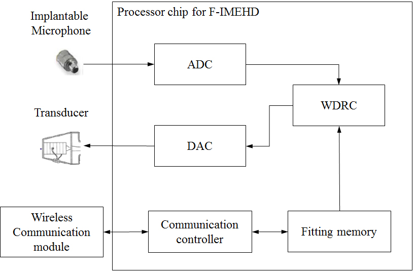
The F-IMEHD comprises an implantable microphone, a transducer, and a wireless communication module. The implantable microphone receives the sound that the user wishes to hear coming from outside the body. The sound received by the microphone is then converted into an electrical signal and is inputted to the chip. The input signal is converted to a digital signal using an analog-to-digital convertor (ADC). The WDRC is used to compress and amplify the input signal based on the extent of hearing loss of the user. The compression and amplification criteria are determined using the fitting algorithm, which are recorded in the fitting memory. In an air-conduction type hearing aid, the fitting operation is performed via wire communication; however, a wireless communication is required for the F-IMEHD, because the components of the F-IMEHD are located in the body. The processed signal, based on the extent of hearing loss, is then converted to an analog signal and is inputted to the transducer. The vibration of the transducer allows the user to hear the appropriately amplified sound.
2.1Modification of the FFT algorithm
Generally, the FFT or a filter bank is used to separate the frequency channels in the WDRC. The advantage of the FFT algorithm is that the signal delay time is less; however, the disadvantage is the high computational complexity. In contrast, the filter bank method exhibits low computational complexity and long delay time. We suggest an FFT algorithm modified without using the phased information of the twiddle factor to reduce the computational complexity. The equation for an N point FFT can be expressed as follows:
(1)
Here,
(2)
The formula is inverse FFT, similar to Eq. (3) [35, 36]:
(3)
The characteristics of the twiddle factor are the same as that expressed in Eq. (4).
(4)
The input data
(5)
We designed a 64-point FFT module using the modified FFT algorithm. Hence,
Figure 3.
Simulation results obtained using the original FFT method: (a) input signal, (b) FFT results using the original method, (c) IFFT results using the original method, and (d) cross correlation with input signal and IFFT results using the original method.
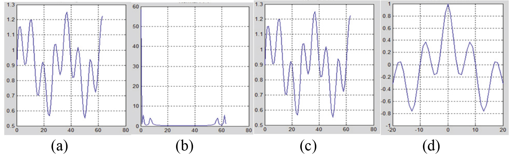
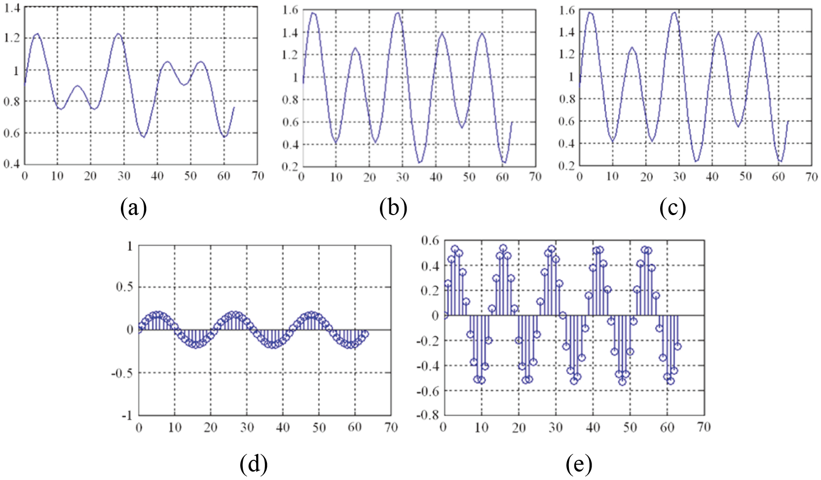
Figure 4.
Simulation results obtained using the proposed FFT method: (a) input signal, (b) FFT results obtained using the proposed method, (c) IFFT results obtained- using the proposed method, and (d) cross correlation with input signal and IFFT results obtained using the proposed method.
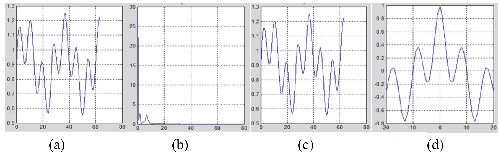
The input signal was mixed comprising sinusoidal signals with magnitudes of 1.1 kHz and 177.8 mV and 3.7 kHz and 177.8 mV, as shown in Figures 3a and 4a. The bias point was 900 mV. In this simulation, the IFFT and cross correlation results of the original and proposed methods were similar.
2.2Design and simulation of a signal processor
The designed processor comprises the WDRC, fitting memory, communication control part, and pulse density modulator. Figure 5 shows the block diagram.
Figure 5.
Block diagram of the designed signal processor for the F-IMEHD.
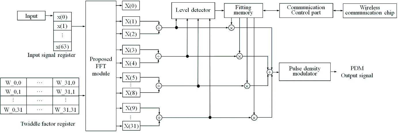
The proposed FFT algorithm comprises 64 channels. Hence, the total input is designed to store 64 channels ranging from
The channels of the WDRC were divided into four based on the vibration characteristics of the electromagnetic transducer. The ranges of channels 1, 2, 3, and 4 were 0.1–1, 1.1–2, 2.1–4, and 4.1–8 kHz, respectively. The twiddle factors based on the frequency of each channel were calculated in advance and applied to the proposed algorithm. The channel segmentation, gain application, and time-domain signal restoration pertaining to the proposed algorithm were simulated using MATLAB (MathWorks, USA). Figures 6 and 7 show the simulation results.
Figure 6.
Simulation results of channel separation: (a) input signal, (b) separated signal on channel 1, (c) separated signal on channel 2, (d) separated signal on channel 3, and (e) separated signal on channel 4.
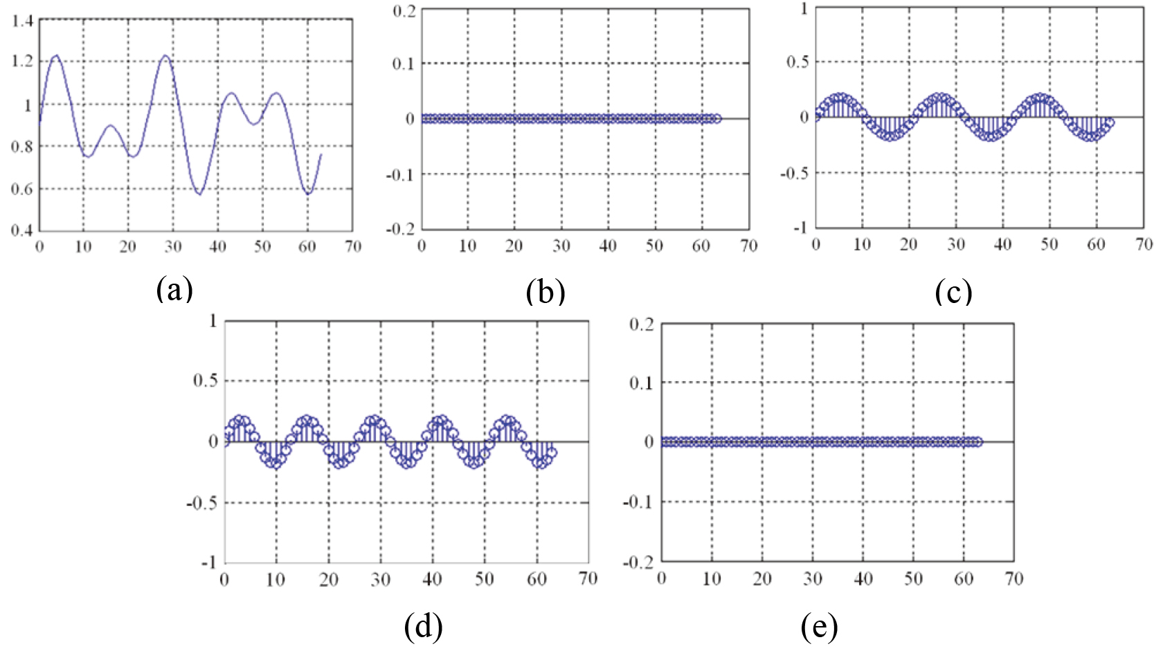
Figure 7.
Simulation results of gain-applied IFFT: (a) input signal, (b) result of applying gain to input signal, (c) result of gain-applied IFFT using proposed method, (d) gain signal applied to channel 2, and (e) gain signal applied to channel 3.
The input signal was mixed comprising sinusoidal signals with magnitudes of 2.5 kHz and 177.8 mV and 3.5 kHz and 177.8 mV, as shown in Figs 6a and 7a. The bias point was 900 mV. In this simulation, the signals with frequencies of 2.5 and 3.5 kHz were separated into channels 2 and 3, respectively, as shown in Figs 6b–e. The gain of channels 1, 2, and 4 was 1, and the gain of channel 3 was 2. Figures 7d and e show the gains applied to channels 2 and 3. The IFFT signal obtained using the proposed method and the mixed signal comprising the sinusoidal signals (2.5 kHz, 177.8 mV and 3.5 kHz, 355.6 mV) were the same, as shown in Fig. 7b and c.
The PDM is a modulation technique in which an analog signal can be expressed in the form of a binary digital signal and is generally used as an output coding method for a hearing aid chip attached to a receiver or an electromagnetic transducer. In the designed signal-processing device, the sampling rate of the input signal is 32 kHz and the output signal of the proposed modified FFT method is also outputted at 32 kHz. Thus, the PDM signal outputted at 64 kHz is selected as the final output signal using a linear interpolation method.
2.3Design and fabrication of the chip
To fabricate the chip, the proposed processor was designed using Verilog-HDL codes. The design results of the Verilog-HDL were verified via simulation using Modelsim-PE 10.3 (Mentor graphics, USA). Figure 8 shows the simulation results.
Figure 8.
(a) Simulation results of the designed processing chip, and (b) enlarged graph on time axis of (a).
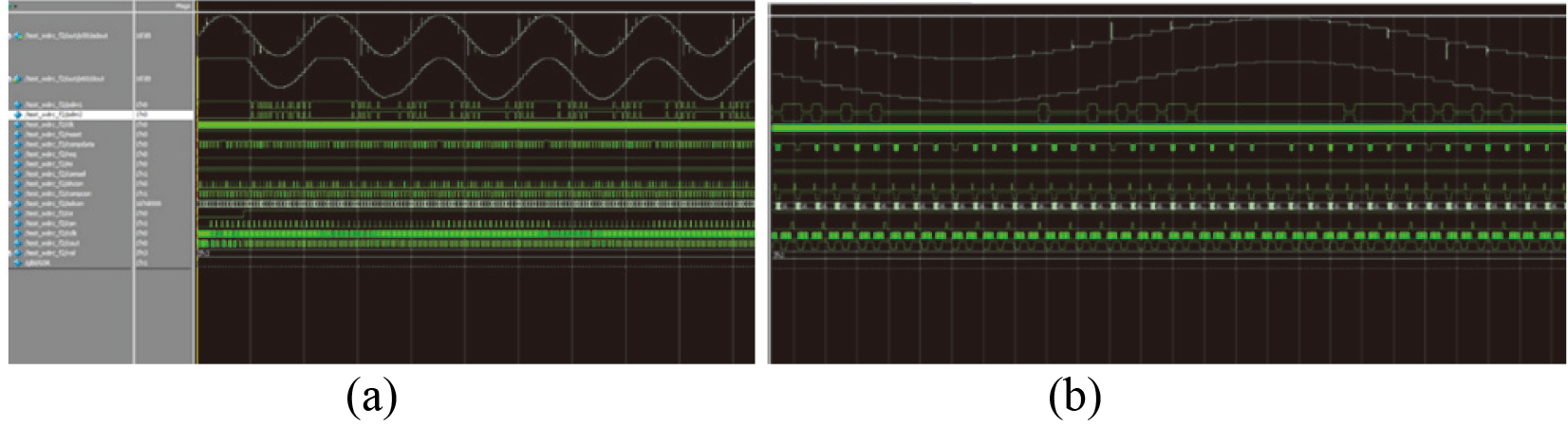
The input signal is an ADC output signal for sinusoidal input of 1 kHz, 90 dBSPL and the gain of all channels is assumed to be 1. There was a time delay of 8 us as shown in Fig. 8a, but this is very short time compared to the time delay of other systems [40].
An SAR ADC and a class-D amplifier were inserted inside the fabricated chip for operating test of the designed processor. Figure 9 is the circuit of SAR ADC and class-D amplifier.
Figure 9.
The circuit of (a) SAR ADC and (b) class-D amplifier using Cadence spectre.
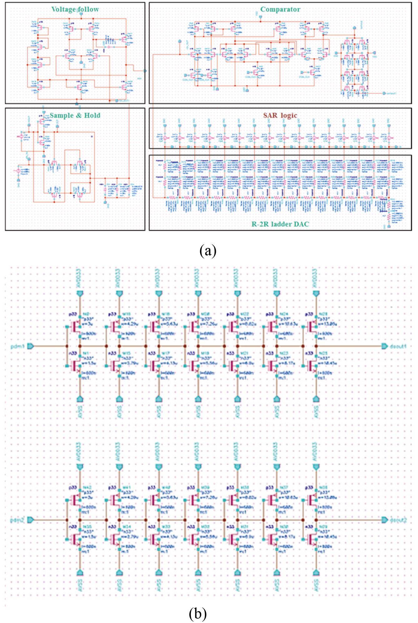
The designed SAR ADC include sample & hold, voltage follow, SAR logic and comparator as shown in Fig. 9a. The voltage follow used for voltage stabilization of sample & hold output. The class-D amplifier was designed to minimize propagation delays using a fixed taper buffer strategy. Figure 10 is layout of SAR ADC and class-D amplifier.
Table 1
Specifications of the fabricated processing chip
| Specification | Value |
|---|---|
| Die chip size | 2.1 mm |
| Packaged chip size | 6.0 mm |
| Number of gates | 190,469 |
| Supply voltage | |
| Core | 1.8 V |
| Digital I/O | 3.3 V |
| Analog | 1.8 V |
| Power consumption of core (simulation) | 0.13 mW |
| Total current consumption at maximum output | 10 mA |
| Package type | 48 pin QFN |
Figure 10.
The layout of (a) SAR ADC and (b) class-D amplifier using Cadence Virtuoso.
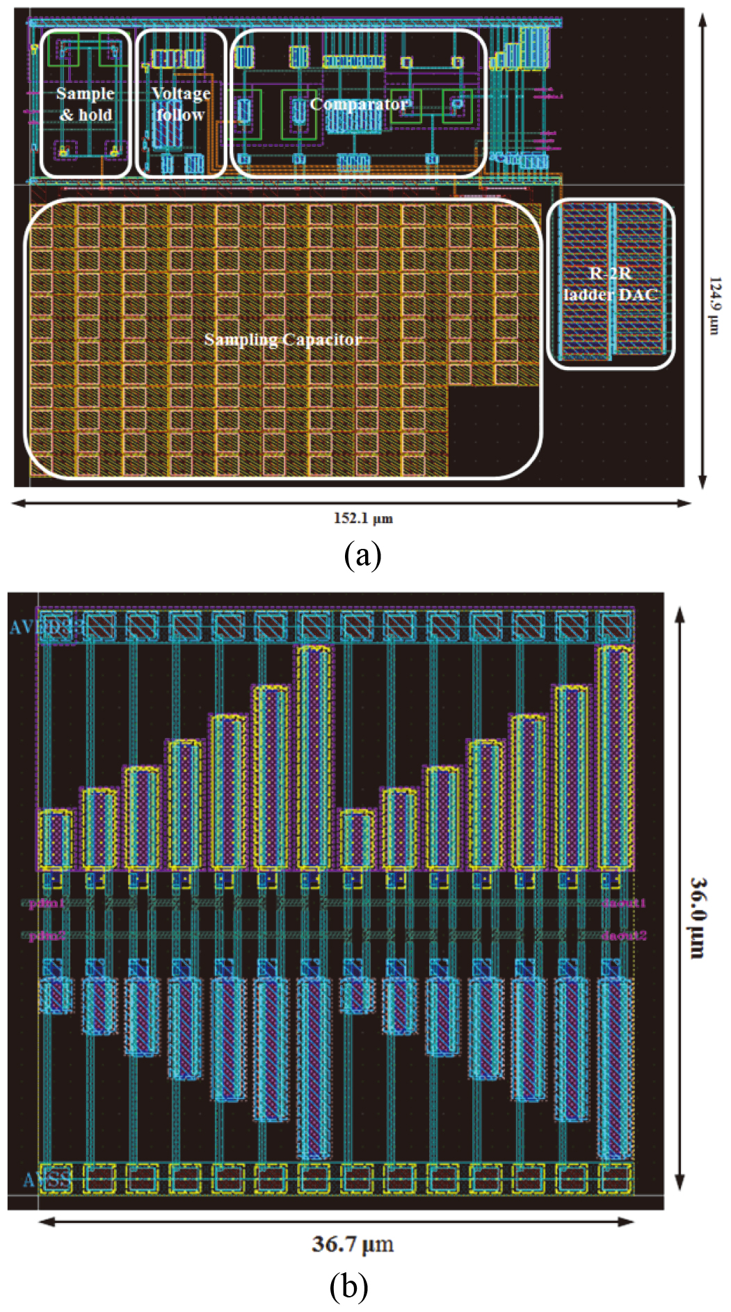
The SAR ADC and class-D amplifier were designed by Virtuoso (Cadence, USA). The size of designed SAR ADC was 124.9
The digital processors designed with Verilog-HDL verified the logic algorithm using the Design Compiler (Synopsys, USA).
The processor chip was designed using Cadence EDA tools. The entire chip, including SAR ADC, class-D amplifier and WDRC, was designed by Virtuoso. Figure 11 is the layout of designed chip.
Figure 11.
The layout of designed chip using Cadence Virtuoso.
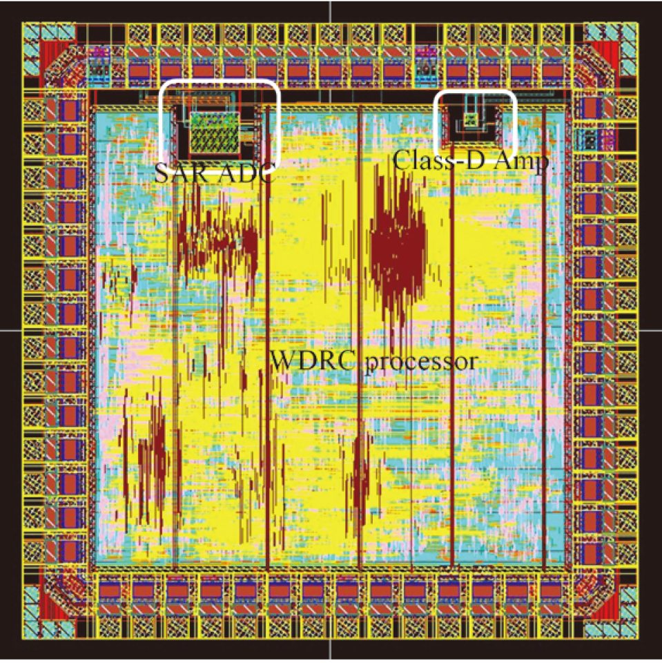
Figure 12.
(a) fabricated die chip micrograph, (b) top of packaged chip, and (c) bottom of packaged chip.
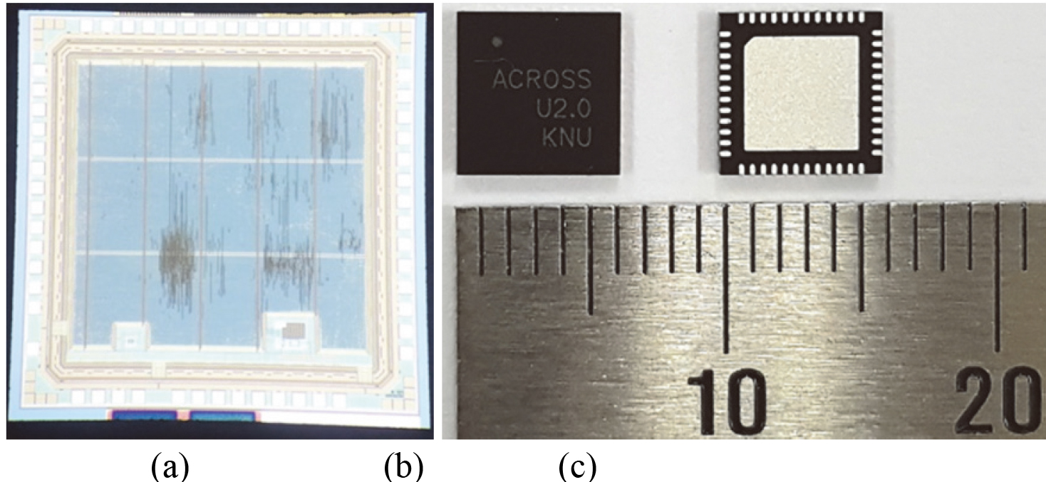
The chip was fabricated using a 0.18
3.Experiments and results
3.1Performance verification of the fabricated processor chip
To verify the performance of the fabricated chip, the vibration characteristics of the electromagnetic transducer were compared with the two input signals. One of the inputs was the signal outputted from the function generator and the other was the signal outputted from the proposed chip. A test board was prepared for the experiment. Figure 13a and b show the schematic and image pertaining to the chip performance experiment, respectively. Figure 14 shows the experimental results.
Figure 13.
(a) Schematic of the experiment, and (b) Image of the experiment.
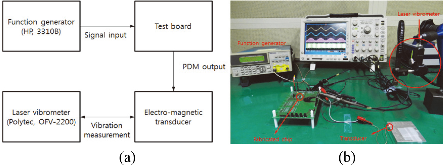
Figure 14.
Experimental results.
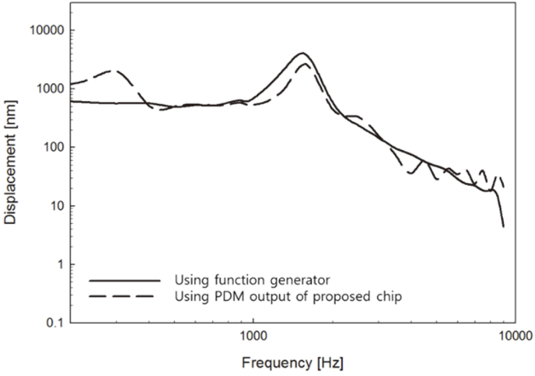
The output signal of the function generator (HP, 3310B) was sinusoidal with a peak of 300 mV. The vibration characteristics of the electromagnetic transducer were measured using a laser vibrometer (Polytec, OFV-2200). The vibration characteristics of the electro-magnetic transducer were similar when the output of the function generator was directly connected and when the PDM output of the proposed chip was connected.
3.2Experiments on human cadaver
Experiments were performed on a human cadaver to verify the applicability of the fabricated chip on the implantable hearing device. The F-IMEHD prototype including the implantable microphone, electro-magnetic transducer, and minimized test board was placed on a human cadaver. Figure 15 shows the images of the implemented prototype and the experiment. Figure 16 shows the experimental results.
Figure 15.
Images of (a) prototype system, (b) minimized test board, and (c) human cadaver experiments.
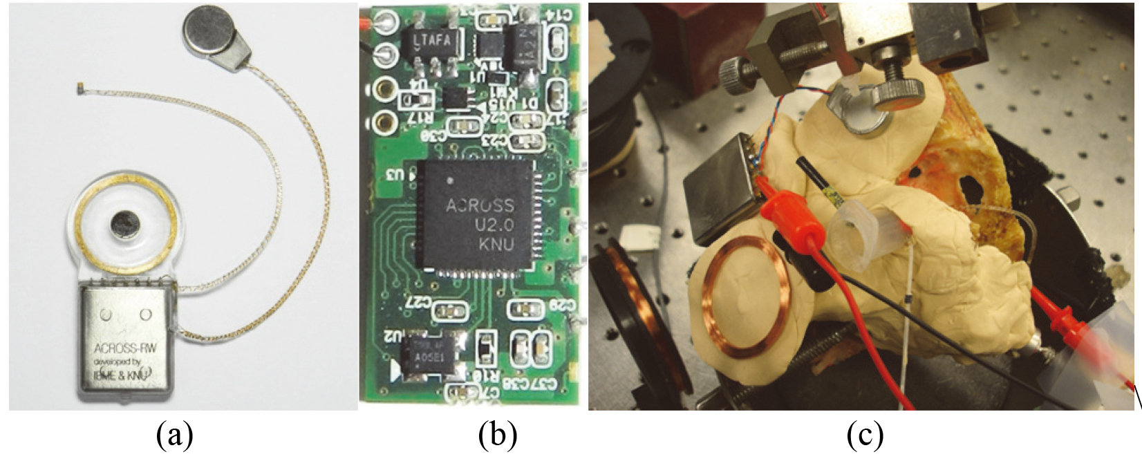
Figure 16.
Results of human cadaver experiments; (a) basic output characteristic with no gain, (b) comparison of gain characteristic for normal hearing loss and 50 dB hearing loss by FIG6 fitting rule.
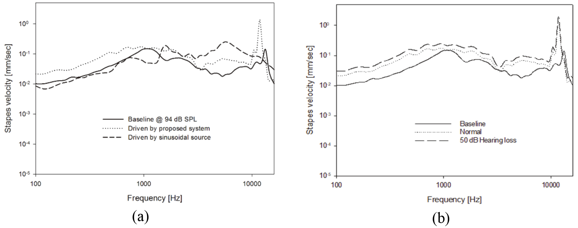
The baseline was the stapes velocity obtained via acoustic stimulation of 94 dB sound pressure level (SPL), as shown in Fig. 16a. The baseline measurement results were used to confirm that the proposed prototype, installed on the cadaver, functioned normally during the experiment. To confirm the normal operation of the implanted transducer, a sinusoidal signal was applied to the implanted transducer, and the stapes velocity was then measured. From this measurement, it was confirmed that the transducer was correctly implanted. Finally, the stapes velocity was measured using the implemented prototype. The results were confirmed to be similar to the stapes velocity produced via sound stimulation, sinusoidal signal, and output signal of the implemented prototype with 94 dB SPL input sound. In addition, we fitted the implemented chip for 50 dB hearing loss from 2 kHz to 10 kHz. The hearing compensation was calculated by FIG6 fitting rule. The FIG6 rule procedure specifies how much gain is required to normalize loudness, at least for medium-and hig-level input signals [1]. The stapes velocity increased about 3.02 dB as shown in Fig. 12b. The performance of implemented chip was confirmed from this experiment results.
4.Discussion and conclusion
This study designed and implemented a signal-processing chip with a small size and a low power consumption for the F-IMEHD system. The implemented chip comprises a multi-channel WDRC, a fitting memory, a wireless communication control part, and an output stage. A modified FFT algorithm was proposed for the WDRC. The digital system was designed using Verilog-HDL codes and verified using Modelsim-PE 10.3 (Mentor graphics, USA). The designed chip was implemented using a 0.18
Table 2
Comparison of the implemented chip with other studied chips
| Chip | Kim’s chip | Gata’s chip | Lan Dai’s chip | Our chip |
|---|---|---|---|---|
| Power consumption [ | 107(Except receiver) | 270 (No signal condition) | 89 | 33,000 (Maximum output) |
| Voltage [V] | 0.9 | 1.1 | 1 | 3.3 |
| Current [mA] | 0.133 | 0.27 | 0.089 | 10 |
| Chip size [mm | 3.744 | 12 | 1.127 | 4.41 |
| Function block | ADC, DAC, DSP, Receiver driver | ADC, DAC, DSP, Receiver driver | OTA, Comparator, AGC | ADC, DAC, FFT, WDRC, Receiver driver, Wirelesscommunication control |
Although many studies have been conducted on the implementation of low-power hearing aid processors, there is no study on the implementation of a processor chip for the F-IMEHD. Kim et al. [41] proposed a chip with a total power consumption of 107
In this study, the simulation results show that the total current consumption was 10 mA at a supply voltage of 3.3 V with maximum output. Moreover, the current consumption of the core was 0.13 mW, including the operating current of the transducer. In the F-IMEHD, an electromagnetic transducer is generally used. The electromagnetic transducer comprises a permanent magnet and a coil. The resistance of the electromagnetic transducer is in the range of 50–300
The experiments performed on the cadaver confirm that the implemented chip has sufficient functional performance. Therefore, the proposed processor can be implemented on a ASIC chip and helps in improving the performance of the F-IMEHD system. We are trying to carry out the human clinical trial to implant implemented hearing aids in the near future. It expected that the main research will be the study for performance improvement for recognition of speech using obtained human clinical trial data.
Acknowledgments
This research was supported by the National Research Foundation of Korea (NRF) grant funded by the Korean government (MSIP) (Nos NRF-2019R1A2C2004347 and 2017R1D1A1B03031388).
Conflict of interest
The authors declare that there is no conflict of interest regarding the publication of this paper.
References
[1] | Dillon H. Hearing Aids. Sydney: Boomerang Press; (2001) . |
[2] | Pollack MC, Carhart R. Amplification for the Hearing Impaired. Orlando: Grune & Stratton Incorporation; (1988) . |
[3] | Kates JM. Digital Hearing Aids. San Diego: Plural Publishing Incorporation; (2008) . |
[4] | Kochkin S. MarkeTrak VIII: Consumer satisfaction with hearing aids is slowly increasing. Hearing Journal. (2010) ; 63: (1): 19-32. |
[5] | Goode R, Rosenbaum M, Maniglia A. The history and development of the implantable hearing aid. The Otolaryngologic Clinics of North America. (1995) ; 28: (1): 1-16. |
[6] | Ko WH, Zhu WL, Maniglia AJ. Engineering principles of mechanical stimulation of the middle ear. The Otolaryngologic Clinics of North America. (1995) ; 28: (1): 29-41. |
[7] | Suzuki J, Shono H, Koga K, Akiyama T. Early studies and the history of development of the middle ear implant in Japan. Advances in Audiology. (1998) ; 4: : 1-14. |
[8] | Kim HH, Barrs DM. Hearing aids: A review of what’s new. Otolaryngology-Head and Neck Surgery. (2006) ; 134: (6): 1043-50. |
[9] | Chasin M. Current trends in implantable hearing aids. Trends in Amplification. (1997) ; 2: (3): 84-107. |
[10] | Dormer KJ, Bryce GE, Hough JV. Selection of biomaterials for middle and inner ear implants. The Otolaryngologic Clinics of North America. (1995) ; 28: (1): 17-21. |
[11] | Hodges AV, Balkany TJ. Cochlear implants for sensorineural hearing loss. Hospital Physician. (2002) ; 38: (10): 22-8. |
[12] | Ramsden RT. Cochlear implants and brain stem implants. British Medical Bulletin. (2002) ; 63: (1): 183-93. |
[13] | Tjellstrom A, Hakansson B. The bone-anchored hearing aid: Design principles, indications, and long-term clinical results. TheOtolaryngologic Clinics of North America. (1995) ; 28: (1): 53-72. |
[14] | Backous DD, Duke W. Implantable middle ear hearing devices: Current state of technology and market challenge. Current Opinion in Otolaryngology & Head and Neck Surgery. (2006) ; 14: (5): 314-8. |
[15] | Haynes DS, Young JA, Wanna GB, Glasscock ME. Middle ear of implantable hearing devices: An overview. Trends in Amplification. (2009) ; 13: (3): 206-14. |
[16] | Silverstein H, Atkins J, Jr., Thompson JH, Gilman NH. Experience with the SOUNDTEC implantable hearing aid. Otology and Neurotology. (2005) ; 26: (2): 211-7. |
[17] | Jenkins HA, Niparko JK, Slattery WH, Neely JG, Fredrickson JM. Otologics middle ear transducer ossicular stimulator: performance results with varying degrees of sensorineural hearing loss. Acta Oto-Laryngologica. (2004) ; 124: (4): 391-4. |
[18] | Bruschini L, Forli F, Passetti S, Bruschini P, Berrettini S. Fully implantable Otologics MET Carina™device for the treatment of sensorineural and mixed hearing loss: Audio-otological results. Acta Oto-Laryngologica. (2010) ; 130: (10): 1147-53. |
[19] | Klein K, Nardelli A, Stafinski T. A systematic review of the safety and effectiveness of fully implantable middle ear hearing devices: the carina and esteem systems. Otology & Neurotology. (2012) ; 33: (6): 916-21. |
[20] | Fisch U, Cremers CW, Lenarz T, Weber B, Babighian G, Uziel AS, et al. Clinical experience with the Vibrant Soundbridge implant device. Otology and Neurotology. (2001) ; 22: (6): 962-72. |
[21] | Kroll K, Grant IL, Javel E. The Envoy®totally implantable hearing system, St. Croix Medical. Trends in Amplification. (2002) ; 6: (2): 73-80. |
[22] | Bankaitis AU, Fredrickson JM. Otologics middle ear transducerTM (METTM) implantable hearing device: Rationale, technology, and design strategies. Trends in Amplification. (2002) ; 6: (2): 53-60. |
[23] | Envoy Medical Corporation, Esteem®Totally Implantable Middle Ear Hearing System (PMA P090018), (2009) . |
[24] | Jenkins HA, Atkins JS, Horlbeck D, Hoffer ME, Balough B, Arigo JV, et al. U.S. Phase I preliminary results of use of the Otologics MET fully implantable ossicular stimulator. Otolaryngology-Head and Neck Surgery. (2007) ; 137: (2): 206-12. |
[25] | Seong KW, Kim MW, Lee JH, Kim MN, Cho JH. Design of a new vibration transducer for implantable middle ear hearing devices. IEEJ Transactions on electrical and electronic engineering. (2010) ; 5: (5): 608-10. |
[26] | Lee JH, Seong KW, Jung ES, Lim HG, Kim MW, Lee JW, et al. Development of a fully-implantable middle ear hearing device in Korea. Hearing Research. (2010) ; 263: (1-2): 247. |
[27] | Siegert R, Mattheis S, Kasic J. Fully Implantable Hearing Aids in Patients With Congenital Auricular Atresia. The Laryngoscope. (2007) ; 117: : 336-40. |
[28] | Cho JH, Park IY, Lee SH. Development of fully implantable middle ear hearing devices with differential floating mass transducer: current status. Journal of Biomedical Engineering Research. (2005) ; 26: (5): 309-17. |
[29] | Puder H. Hearing aids: an overview of the state-of-the-art, challenges, and future trends of an interesting audio signal processing application. Proceedings of 6th international symosium on IEEE Image and Signal Processing and Analysis; (2009) : 1-6. |
[30] | Schneider T, Brennan R. A multichannel compression strategy for a digital hearing aid. IEEE International Conference on Acoustics. Speech and Signal processing. (1997) ; 1: : 411-4. |
[31] | Van Buuren RA, Festen JM, Houtgast T. Compression and expansion of the temporal envelope: evaluation of speech intelligibility and sound quality. Journal of the acoustical society of America. (1999) ; 105: : 2903-13. |
[32] | Keidser G, Grant F. The preferred number of channels (one, two, or four) in NAL-NL1 prescribed wide dynamic range compression (WDRC) devices. Ear and hearing. (2001) ; 22: (6): 516-27. |
[33] | Hung GK. Biomedical Engineering Principles of the Bionic Man. Singapore: World Scientific; (2009) . |
[34] | Kim DW, Seong KW, Kim MN, Cho JH, Lee JH. A 1-channel 3-band wide dynamic range compression chip for vibration transducer of implantable hearing aids. Bio-Medical Materials and Engineering, (2014) ; 24: (1): 1009-17. |
[35] | Oppenheim AV, Schafer RW. Discrete-time signal processing, New jersey: Prentice hall; (2009) . |
[36] | Proakis JG, Manolakis DG. Digital signal processing principles, algorithms, and applications, New jersey: Prentical hall; (2007) . |
[37] | Sorensen HV, Jones DL, Heideman MT, Burrus CS. Real-valued fast Fourier transform algorithms. IEEE Trans. Acoust. Speech Sig. Processing. (1987) ; 35: (6): 849--63. |
[38] | http://www.ti.com, Texas Instruments, USA. |
[39] | http://www.nordicsemi.com, Nordic semiconductor, Norway. |
[40] | Alexander J. Hearing Aid Delay and Current Drain in Modern Digital Deives. Canadian Audiologist. (2019) ; 3: (4). |
[41] | Kim SY, Lee SJ, Cho NJ, Song SJ, Yoo HJ. A Fully Integrated Digital Hearing Aid Chip With Human Factors Considerations. IEEE JOURNAL OF SOLID-STATE CIRCUITS, (2008) ; 43: (1): 266-74. |
[42] | George Gata D, Sjursen W, James RH, John WF, Lieyi F, Gerald RI, et al. A 1.1-V 270-uA Mixed-Signal Hearing Aid Chip, Ieee Journal Of Solid-State Circuits, (2002) ; 37: (12): 1670-8. |
[43] | Dai L, Chen C. A 69-dB SNR 89-μW AGC for Multifrequency Signal Processing Based on Peak-Statistical Algorithm and Judgment Logic. VLSI Design, (2016) ; 2016: : 7. |
[44] | Shin DH, Seong KW, Puria S, Lee KY, Cho JH. A tri-coil bellows-type round window transducer with improved frequency characteristics for middle-ear implants. Hearing Research. (2016) ; 341: : 144-54. |
[45] | Kim MK, Yoon YH, Park IY, Cho JH. Design of differential electromagnetic transducer for implantable middle ear hearing device using finite element method. Sensors and Actuators A, (2006) ; 130: : 234-40. |