
Using a PIM interface for improving computer medical image processing abilities
Abstract
BACKGROUND:
Biomedical engineers in particular require fast and powerful data processing systems to process computerized tomography and magnetic resonance imaging scans and other medical imaging technologies. However, current computer data processing technologies are unable to satisfy such requirements. A promising approach to addressing these limitations is processing in memory (PIM). Unfortunately, several issues, such as the compatibility and interconnection of PIM with legacy systems, still remain.
OBJECTIVE:
This paper proposes a standard memory bus-based PIM interface for medical image processing and a PIM platform. The proposed PIM interface can overcome problems of compatibility with legacy systems.
METHODS:
We will adapt an embedded system based on a commercial application processor (AP) to a medical image system to verify the functions and the performance of the proposed PIM interface. Using the PIM platform, we apply the proposed PIM interface and the AP to execute an image processing program, measure the image processing times, and compare the results of the measurements.
RESULTS:
Experimental results show that while the functions of the proposed PIM interface are normal, the processing time of PIM is more than 81% faster than that of the AP.
CONCLUSION:
The experimental results prove that the proposed PIM interface is able to solve problems of compatibility with legacy systems. We foresee that not only the medical image processing field but also a number of academic fields and professional sectors will use PIM in their data-intensive applications.
1.Introduction
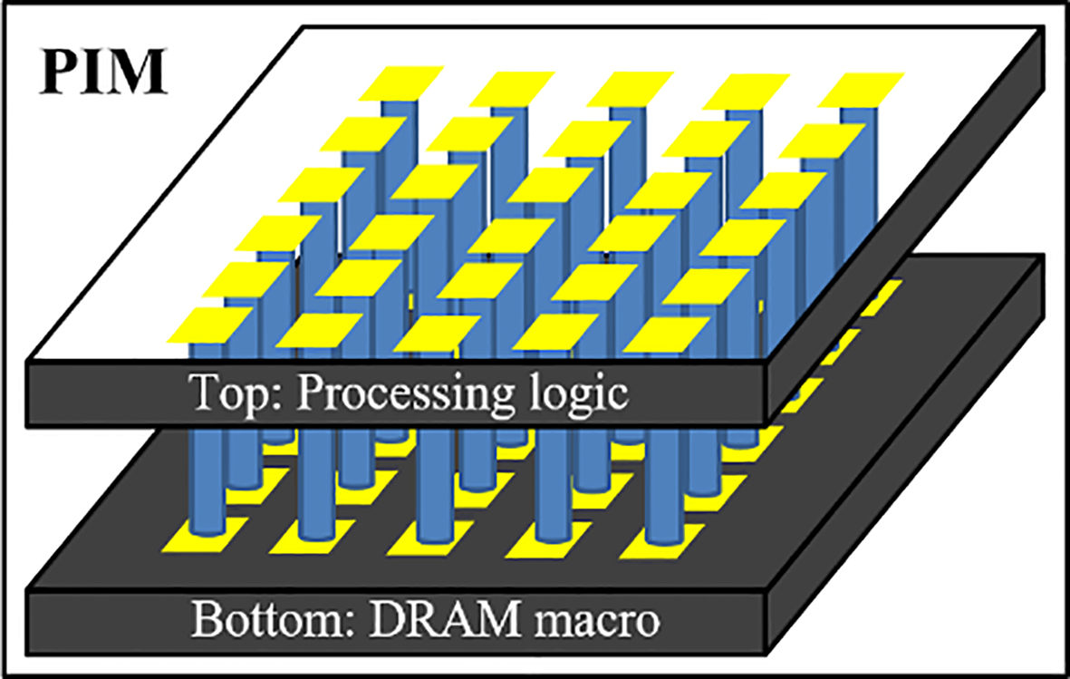
Over the last few years, the volume of data has exploded [1]. The flood of information is the result of individuals accessing a number of social network services to search for high-quality multimedia content, companies accessing innumerable complex data related to potential customers to build their business [2], and many fields such as the public media, the medical industry, the natural and social sciences, the humanities, and engineering using such data to predict and understand various social phenomena [3]. Therefore, application providers must be capable of delivering timely information to their clients from the steady stream of a massive amount of data that accumulate every second of every day [4]. Unfortunately, traditional computing systems are incapable of delivering sufficient computing power to accomplish this task because of the memory wall crisis. The medical industry is particularly impacted because it incorporates the latest computer engineering technology. As a promising approach to overcoming the performance limitations of traditional computing systems, the research community has explored the datacentric computing paradigm [5], specifically, processing in memory (PIM), for use in future computer systems. PIM uses three-dimensional integrated circuit (3D-IC) technologies such as through-silicon vias and fan-out wafer level packaging (FOWLP) [6, 7, 8] to facilitate the stacking of processing logic and memory dies in a single package. It also minimizes data movement by placing the computation close to where the data reside. If existing medical image systems adopt 3D-IC-based PIM, their performance will dramatically improve. Figure 1 illustrates the concept of PIM.
Figure 1.
Basic concept of 3D-IC technology-based processing in memory (PIM).
To date, however, PIM has not yet been realized, for it is unable to address critical issues regarding interconnection and compatibility [5]. In particular, the use of PIM within traditional computer systems requires the establishment of standards related to the interconnection between a host-processor and a PIM subsystem and associated management methods. The existence of established standards could encourage compliance with such standards by the global computer industry. Thus, the purpose of this paper is to address limitations related to the interconnection between PIM and existing computer systems by proposing a standard memory bus-based PIM interface. The paper is organized as follows. Section 2 introduces the motivation of this paper, and Section 3 defines the concept of the proposed PIM interface. Section 4 describes the experimental environment and validates the performance of the proposed interface-based PIM system by comparing the results of experiments and Section 5 concludes the paper.
2.Motivation
To commercialize new computer architectures, we must solve issues of compatibility with legacy systems. PIM is no exception. In terms of the operating system (OS) and computer organization, PIM has several critical limitations related to its integration with existing computer systems. Such limitations include the memory hierarchy, virtual memory, demand paging, and memory interface standards [5, 9]. As the design of PIM, which is a memory, uses dynamic random-access memory (DRAM), it can be employed as the main memory or the external memory. If PIM is used as the main memory in a traditional computer system, typical memory functions such as read and write operations work well, but special functions, that is, arithmetical, conditional, and accelerable operations, may not operate normally. Because of the virtual memory policy of the OS, PIM will distort addresses resulting from the demand paging of the OS and caches in the memory hierarchy, and the unpredicted exact physical addresses of the operands of the special functions [10, 11]. Furthermore, to support PIM operations and to use the special functions of PIM, the interface must be capable of carrying opcodes and operands. Since existing standard-based DRAM interfaces, however, were designed for only basic memory operations, they are not suitable for PIM [12].
One objective of this paper is to study the memory interface of PIM. While most standard DRAM has a fixed latency bus protocol [12], PIM requires a variable latency bus protocol because it has to support various operations whose processing times differ. Therefore, this paper proposes a new memory interface for PIM, the design of which is based on pseudo-static, random-access memory (PSRAM) [13], the standard DRAM interface, and communicated by a variable-latency-based protocol. We use an embedded system-based PIM platform to conduct experiments on the proposed PIM and then evaluate and verify the functions and performance of the PIM interface in various PIM operations and image processing applications.
3.Proposed PIM interface
This section explains the proposed PIM interface, summarizes the PSRAM, and describes the modified PSRAM protocol for PIM and its hardware architecture with additional functionality.
3.1PSRAM
PSRAM is a type of DRAM with circuits for self-refresh and address-decode. Therefore, with regard to the memory controller, PSRAM is controlled in the same way as a static random-access memory (SRAM). Unlike most SRAM, however, PSRAM has a WAIT signal. The refresh of typical DRAMs is operated by the memory controller, but since PSRAM has a built-in refresh logic, the response time of PSRAM is changeable. Thus, the WAIT signal informs what is dealing with a required address and command for the memory controller. Figures 2 and 3 illustrate the basic read and write operations of PSRAM.
![Write timing of PSRAM [13].](https://ip.ios.semcs.net:443/media/thc/2020/28-S1/thc-28-S1-thc209049/thc-28-thc209049-g002.jpg)
![Read timing of PSRAM [13].](https://ip.ios.semcs.net:443/media/thc/2020/28-S1/thc-28-S1-thc209049/thc-28-thc209049-g003.jpg)
The control signals of PSRAM are CLK, ADDRESS, ADV#, CE#, OE#, WE#, WAIT, and DQ, shown in Fig. 2. The ADV# indicates that a value of the ADDRESS is valid. The CE is used as a chip select signal. Since the data bus of PSRAM is bi-directional, the OE# expresses the present direction of the data bus. The WE# indicates that a present request is either read or write, and the WE# and the ADV# are asserted at the same time. As the PSRAM protocol is based on variable latency, the WAIT signal indicates the status of the data bus according to the WE#. Because the WE# is the write mode in Fig. 2, WAIT is asserted when the data bus is able to receive the write data. The DQ, the data bus shown in Fig. 2, illustrates the 4-beat burst transfer and write mode. Figure 3 displays the read timing of PSRAM, which is nearly identical to the write timing shown in Fig. 2. As the PSRAM mode in the figure is read, however, WE# is deasserted when the ADV# is asserted. The OE# is contrary to the write mode of PSRAM.
3.2Proposed protocol for PIM
As the processing logic in PIM works according to a read-modify-write scheme (except for basic memory operations), most PIM operations must be atomic [9]. For atomic operations, a packet format of the PIM operation requires various fields such as an opcode, destination and source addresses, and immediate data. Thus, this paper proposes a format of the PIM operation and a method for transferring the PIM operation based on the PSRAM interface. Figure 4 illustrates the format of the proposed PIM-operations.
Figure 4.
Packet format of PIM operations.
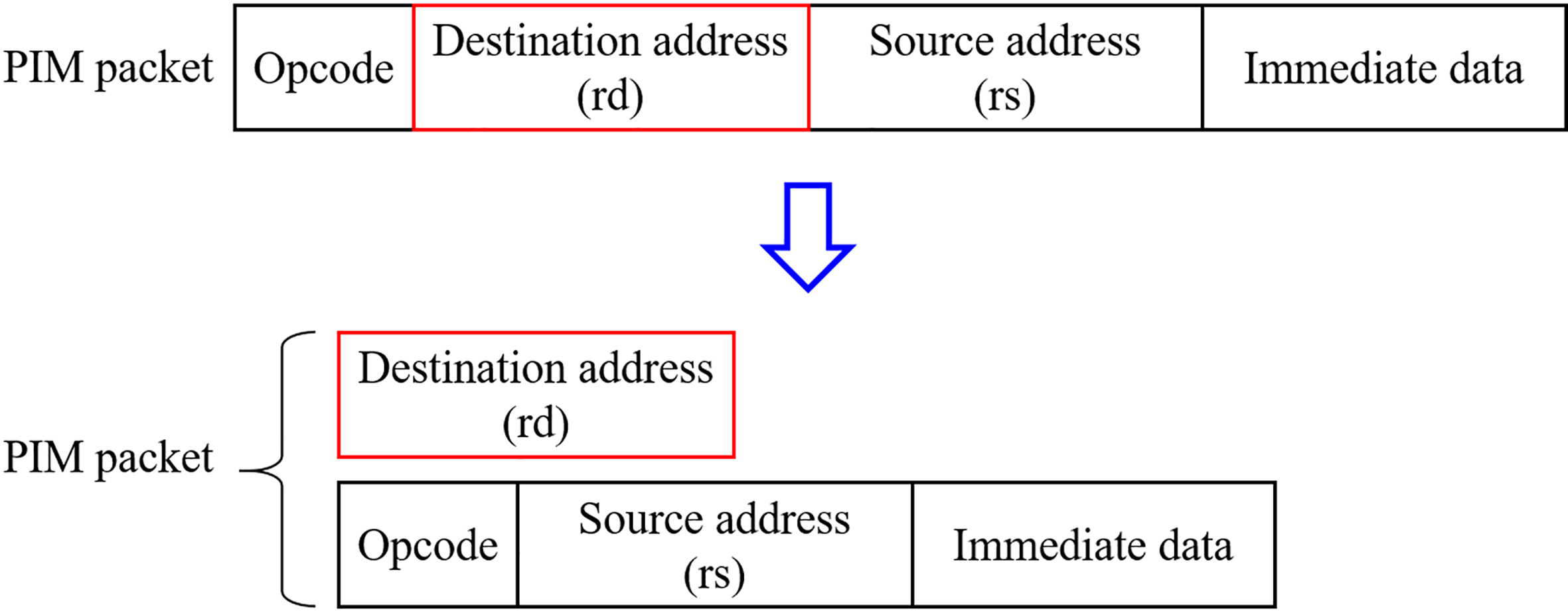
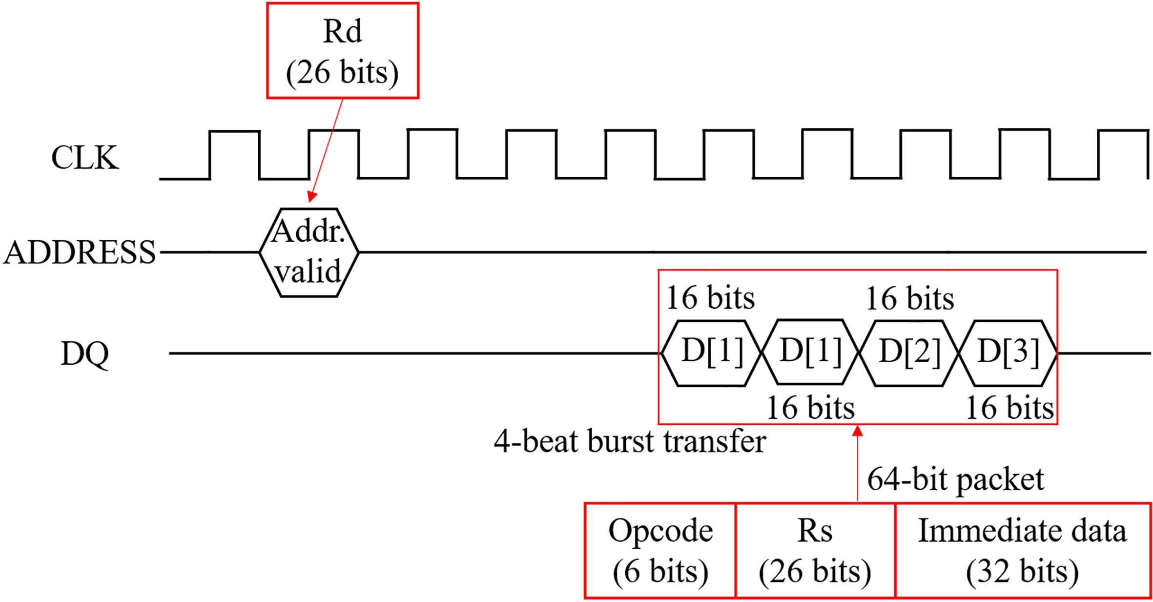
The proposed PIM packet consists of an opcode, a destination address, a source address, and immediate data fields. The opcode field indicates an instruction processed by the processing logic. In basic memory operations, the destination address field is used for read and write addresses. The destination address field, however, can also be used for writing the results of PIM operations. If the instruction in the opcode field is an immediate type, the processing logic uses the value of the immediate field in the PIM packet as the operand for processing an instruction; but if the instruction is a recall type, the processing logic uses the operand loaded from the address of the source address field in the PIM packet. To transfer PIM operations through the PSRAM interface, we separate the destination address field from one PIM packet, shown in Fig. 4. Since the address bus and the data bus of the PSRAM interface are divided, we employ the address bus of the PSRAM interface to transfer destination addresses without modification. To transfer the opcode, the source address, and immediate data, we use the transfer mode of the data bus in the PSRAM interface. Under the assumption that the PIM packet has a fixed length, we omit the packet head and tail fields even though they do not have to be omitted. Figure 5 shows the timing of the proposed PIM interface and protocol.
Figure 5.
Proposed PIM interface and protocol.
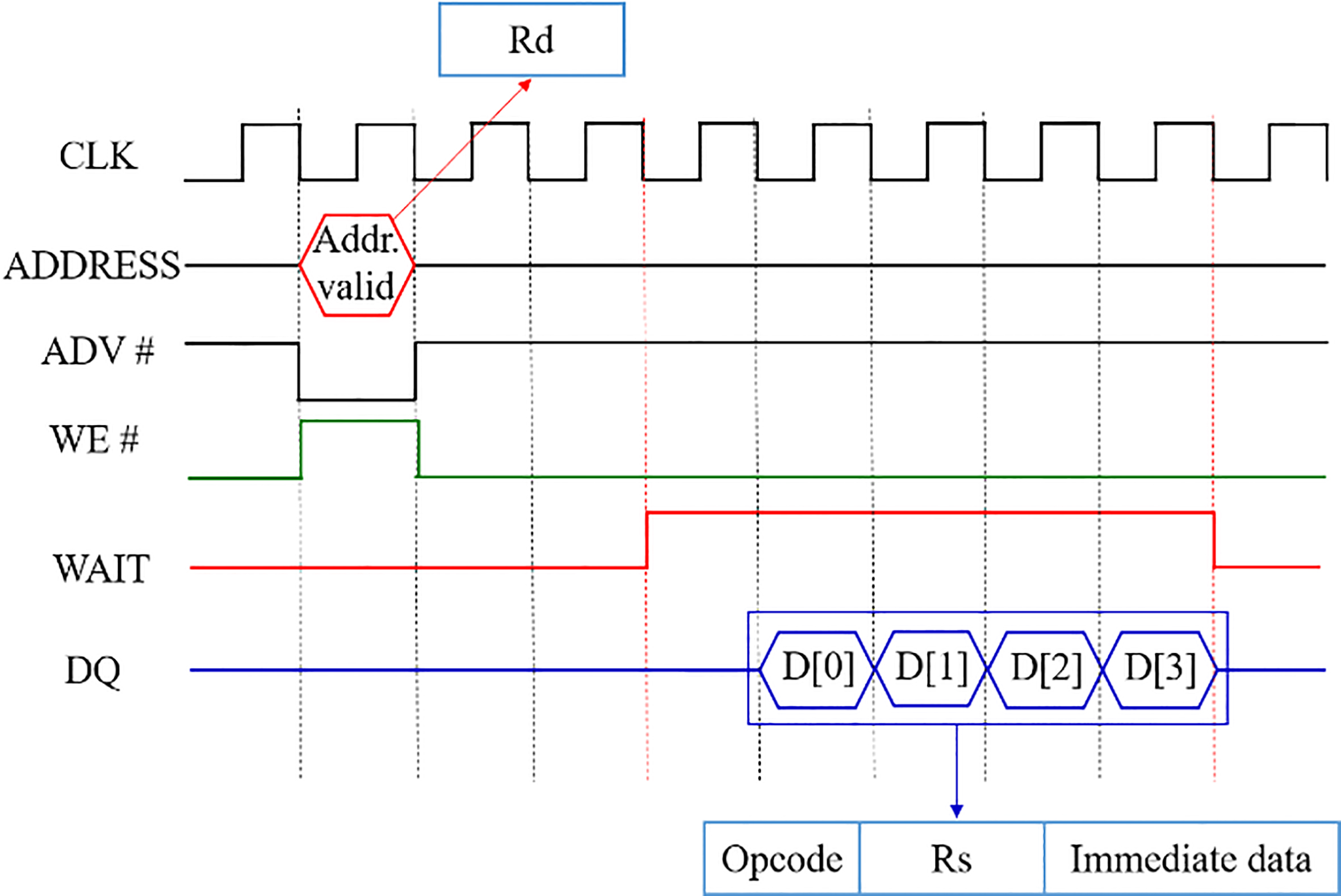
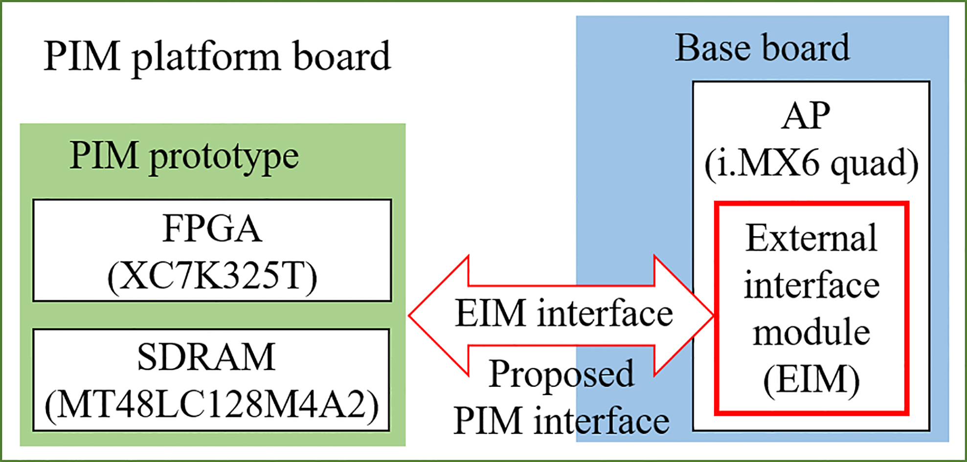
Figure 6.
Block diagram of the PIM platform.
4.Experiments
This section describes the experimental environment and then reports and evaluates the experimental results and performance of the proposed PIM interface.
4.1Experimental environment
To verify the functions and the performance of the PIM interface, we designed an embedded system-based PIM platform that will specifically adapt to medical imaging systems. Figure 6 illustrates a block diagram of the PIM platform. The PIM platform board consists of two parts: a PIM prototype and a base board. The former is a prototype of the 3D-IC-based PIM chip. The FPGA [14] and the SDRAM [15] in the PIM prototype are employed as the processing logic and the DRAM macro in PIM, respectively. A 32-bit commercial application processor (AP) [16] is used as the host processor of the PIM platform. The AP has an external memory channel, referred to as the “external interface module” (EIM). We implement the PIM interface by modifying the PSRAM protocol on the EIM. The bus speed of the EIM in the AP supports a maximum bus speed of 133 MHz, but since we must verify the compatibility with legacy systems and the functions of the proposed PIM interface, we set the EIM bus in the PIM platform at a bus speed of 33.33 MHz.
This study entails the use of 32-MB SDRAM as the internal memory of PIM, and the data bus of the PIM interface in the platform has a 16-bit wide 4-beat burst transfer. Thus, the PIM platform has a destination address of 26 bits and a packet length of 64 bits, a 6-bit opcode, a 26-bit source address, and a 32-bit immediate data packet. Figure 7 shows that the PIM packet is communicated between the PIM prototype and the AP. Because the number of PIM opcodes supported in this paper is limited by hardware resources and the response time, the design of the processing logic allows the processing of simple operations. The opcode list appears in Table 1. The OS in the proposed PIM platform uses a 32-bit embedded Linux.
Table 1
Opcode list of the proposed PIM platform. The Opcode and the Symbol in the headings of the table represent opcode values in PIM-operations supported by the PIM-platform and their symbols, respectively, which symbolize the atomic operations of each PIM operation
| Symbol | Opcode | Description |
|---|---|---|
| WRITE | 6’b00_1111 | Read |
| READ | 6’b01_0000 | Write |
| W_OR_I | 6’b01_0001 | I-type OR and write |
| W_NOR_I | 6’b01_0010 | I-type NOR and write |
| W_XOR_I | 6’b01_0011 | I-type XOR and write |
| W_AND_I | 6’b01_0100 | I-type AND and write |
| W_NAND_I | 6’b01_0101 | I-type NAND and write |
| W_ADD_I | 6’b01_0110 | I-type ADD and write |
| CAWGT_I | 6’b01_0111 | Compare and I-type write if greater than |
| CAWLT_I | 6’b01_1000 | Compare and I-type write if less than |
| CAWEQ_I | 6’b01_1001 | Compare and I-type write if equal |
| CAWZERO_I | 6’b01_1010 | Compare and I-type write if zero |
| W_OR | 6’b10_0001 | R-type OR and write |
| W_NOR | 6’b10_0010 | R-type NOR and write |
| W_XOR | 6’b10_0011 | R-type XOR and write |
| W_AND | 6’b10_0100 | R-type AND and write |
| W_NAND | 6’b10_0101 | R-type NAND and write |
| W_ADD | 6’b10_0110 | R-type ADD and write |
| SORT | 6’b10_0000 | 25-pixel window median-sort and write |
| CONS_SORT | 6’b10_0001 | Median-sort after 25-pixel window shift and write |
Figure 7.
Protocol of the proposed PIM interface in the PIM platform.
4.2Experimental results
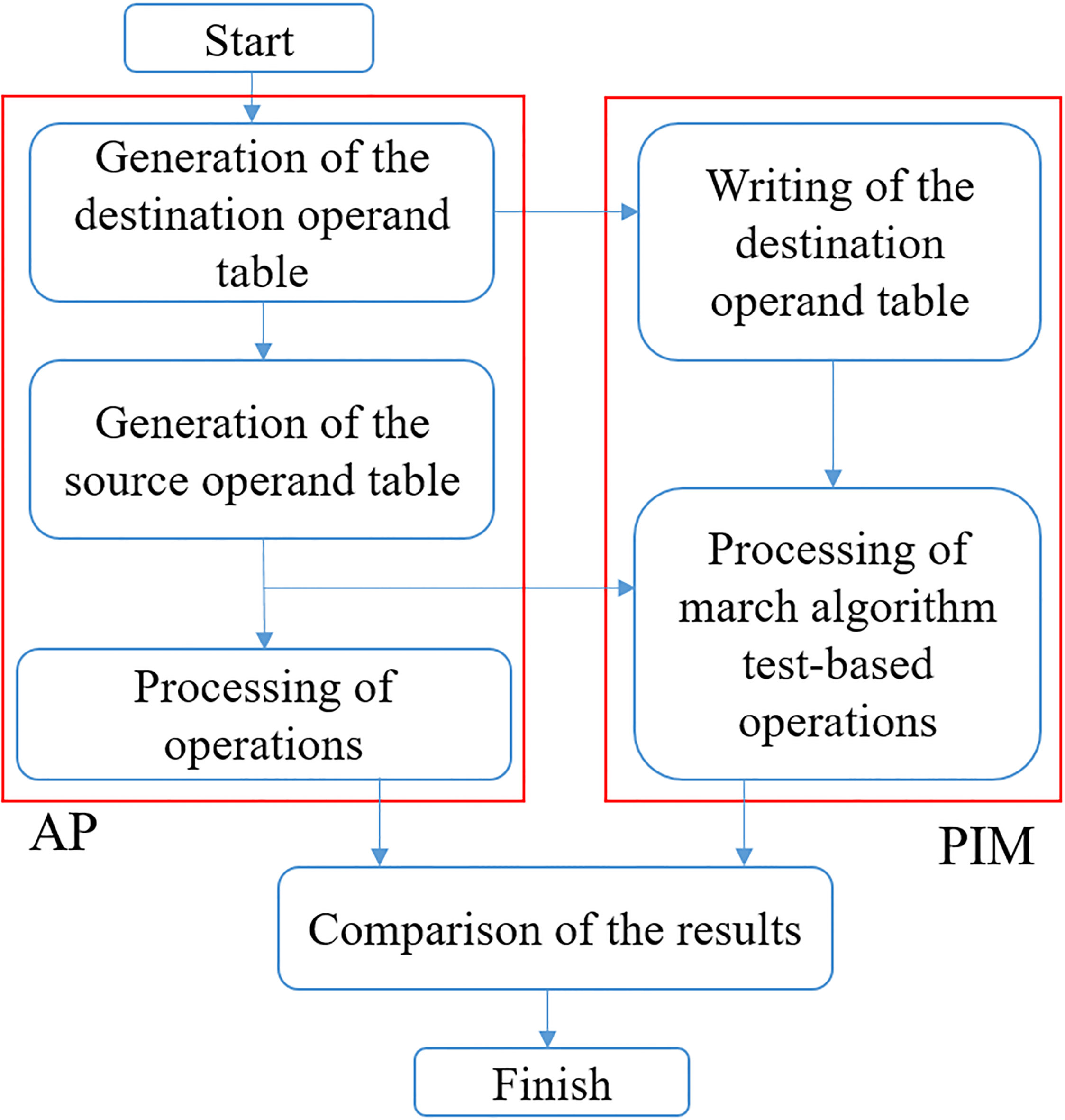
To verify the proposed PIM interface and operations in the proposed PIM, we developed test applications based on MARCH pattern tests on the MARCH algorithm [17]. Furthermore, recent research [18, 19, 20] related to PIM has reported the suitability of data-intensive applications for PIM such as image processing, artificial intelligence, and graph algorithms. Therefore, we implemented median-filtering processed by the AP and the proposed PIM for data-intensive applications. We processed the MARCH algorithm test-based applications as shown in Fig. 8 and generated the destination and source operands as well as the number of PIM entries. Then each PIM operation in Table 1 was executed by the AP and the proposed PIM. To verify the functions of the proposed PIM interface and PIM, we compared their results. During the experiments, problems of compatibility with legacy systems did not occur, so we confirmed that all functions in the proposed PIM and the interface were normal.
Figure 8.
Flowchart of test operations based on the pattern tests from the MARCH algorithm.
To verify the function and the performance of the proposed PIM, we developed two application programs based on the embedded system with the AP: the median-filter algorithm, executed by only the AP and the same algorithm executed by only the proposed PIM. Each program used its own hardware resources to process one standard-processing image and two medical images, both of which were 24-bit color images with a resolution of 512 by 512 pixels.
To evaluate the performance of the PIM interface, this paper executed the median-filter programs on the embedded system-based PIM platform board and used the functions of window API to measure the processing times of each program [21, 22]. Since the median-filter processing procedures of the AP and the proposed PIM differ in a number of ways, the methods of measurement of the processing times of the programs also differ and are diagrammed in Fig. 9.
Table 2
Comparison of the processing times of median filtering by the AP and the PIM. The images denote the subjects of the experiments in this paper. The AP and the PIM symbolize the processing times for median filtering by the AP and the PIM, respectively. The reduction ratios denote the processing times in the PIM resulting from comparisons of the three images from the experiments conducted in this study
| Image | AP (sec.) | PIM (sec.) | Reduction ratio (%) |
|---|---|---|---|
| Lena | 8.004326 | 1.288066 | 83.91 |
| Cancer | 6.719369 | 1.245627 | 81.46 |
| Skin | 7.862324 | 1.287875 | 83.62 |
Figure 9.
Flowcharts for measuring the performance of the AP and the proposed PIM.
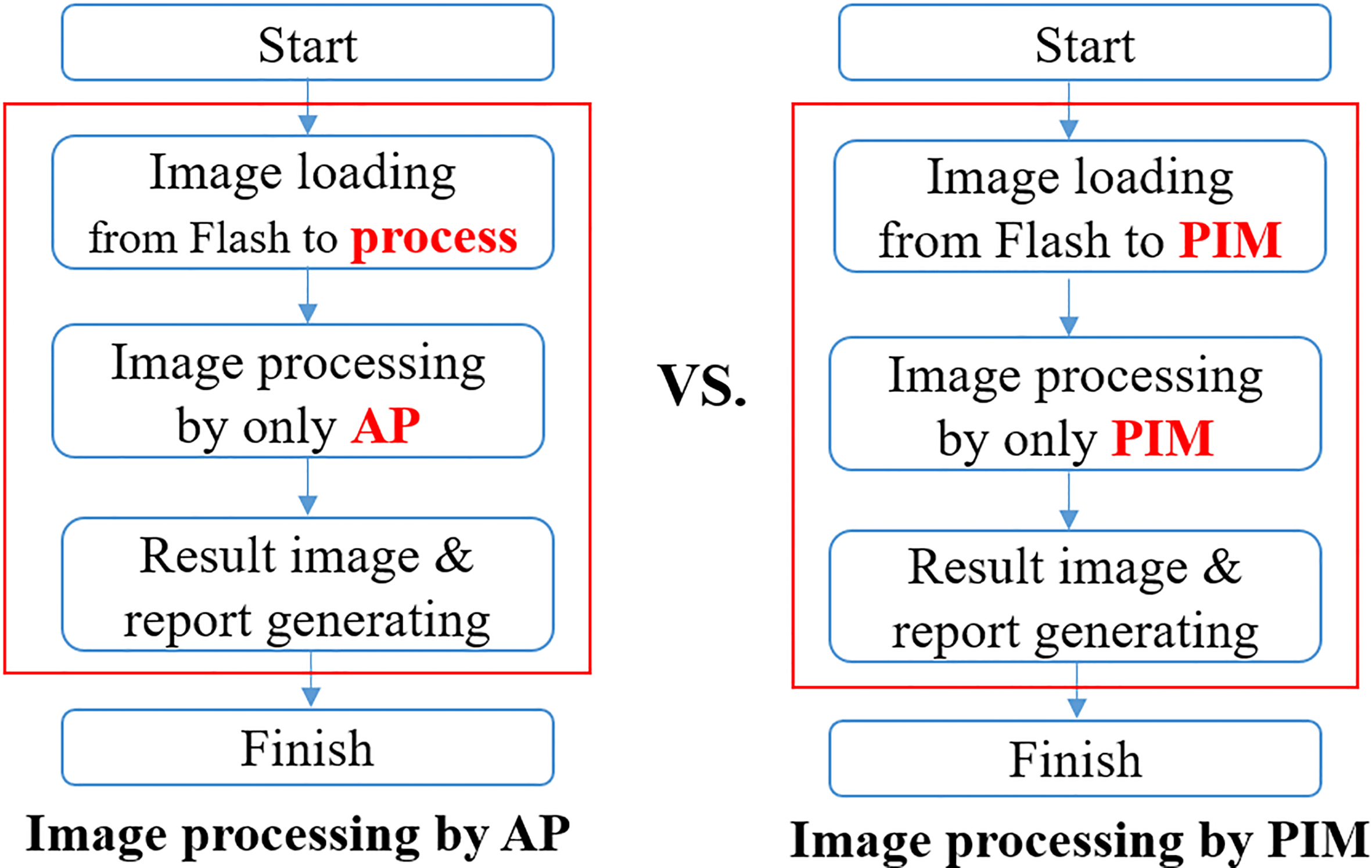
In the case of the AP, the processing time measurement must begin when the test image from the flash memory is loaded into the main memory of the system and end when the resulting image and report files for evaluation are written to the flash memory after median filtering is complete. In the case of PIM, the processing time measurement must begin when the test image from the flash memory is loaded into PIM and end when the resulting image and report files for evaluation are written to PIM after the median filtering is complete. Since a DDR3 is used as the main memory in the PIM platform, and its access time differs from that of the PIM, employing these measuring methods assured the reliability and fairness of the experimental results in this paper.
Figure 10.
Image processing results of the test programs of the AP and the proposed PIM.
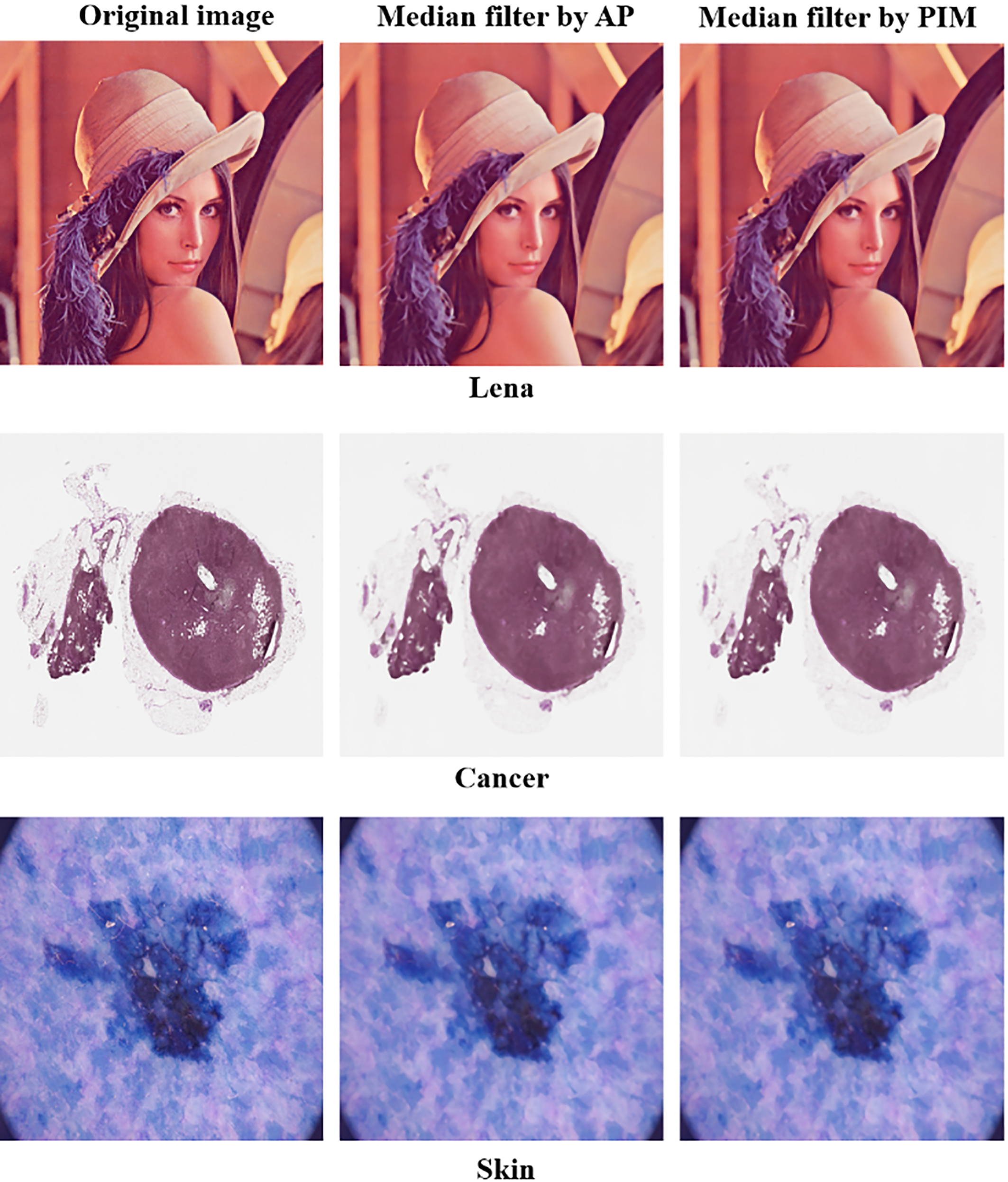
The processing results are displayed in Fig. 10. The experiments in this paper used a woman, Lena, cancer, and skin as source images for the median filtering process [23, 24, 25]. Lena is a standard test image in the field of image processing; the cancer image is provided by the Digital Slide Archive, a software platform for cancer research; and the skin image, which shows pigmented skin lesion, comes from HAM10000. In the resulting images processed by the AP and PIM, the edges resulting from median filtering are smoother than those of the source images. In addition, since the resulting images of median filtering by the AP match those by the PIM, we confirm that the operations performed by the proposed PIM interface and PIM functioned normally.
Table 2 compares the median-filter processing times of the AP and the proposed PIM. To create the images of Lena, cancer, and the skin, the processing times of the AP were 8.004326 secs, 6.719369 secs, and 7.862624 secs, respectively, and those of PIM were 1.288066 secs, 1.245627 secs, and 1.287875 secs, respectively. The processing times of PIM were almost the same, but the results of the AP differ, the reason being that the AP and PIM must repeatedly process a sorting algorithm for processing the median filter [26]. To do so, PIM uses a hardware-sorting module, so the comparators in the sorting module have uniform latency regardless of the results of comparison. The sorting algorithm of the AP, however, is processed by software, and the sorting time is affected by the results of the comparison of the features of the test images. Therefore, the sorting time of the AP is not uniform, and the results of the AP in Table 2 vary widely, showing that the processing time of PIM is more than 81% faster than that of the AP. The explanation for this finding is that most of the median filtering of the PIM was processed by hardware-based processing logic and the internal SDRAM. As a result, the internal memory in the PIM reduced the memory-transaction overhead for accessing pixel data, so the processing logic in the PIM accelerated the median filtering process. We repeated the experiments 100 times. Thus, to mitigate interruptions by the background processes of the OS, we averaged the results from the repeated experiments to determine the overall experimental results.
5.Conclusion
In an effort to design a more efficient data-centric computing paradigm, this paper proposed a PIM interface and protocol by modifying the PSRAM interface and overcame problems of compatibility with legacy systems. To verify the function and the performance of the proposed interface-based PIM, we suggested an embedded system-based PIM platform. In addition, we developed application programs based on the embedded system to evaluate and compare the functions of and performance gaps between a commercial AP and the proposed PIM. Results of the experiments showed that although the images processed by the PIM and the AP were identical, the processing time of the proposed PIM was considerably faster than that of the AP. Although we employed only one application in experiments, we found that the median-filter algorithm, a data-intensive application, was effective for evaluating the proposed PIM. Once this research shows progress, we will explore and develop various applications, particularly those focusing on medical imaging systems, in a future project. Since medical imaging systems belong to a category of traditional computing systems, they are strongly impacted by the memory wall crisis, which limits their efficacy. We foresee that not only the medical image processing field but also a number of academic fields and professional sectors will use PIM in their data-intensive applications.
Acknowledgments
This work was financially supported by the Industrial Strategic Technology Development Program of MOTIE/KEIT (no. 10052653). Also, these are the results of a study on the “Leaders in INdustry-university Cooperation +” Project (no. 2019DG055010101), supported by the Ministry of Education and the National Research Foundation of Korea.
Conflict of interest
None to report.
References
[1] | Brown B, Chui M, Manyika J. Are you ready for the era of big data? McKinsey Quarterly. (2011) ; 4: : 24. |
[2] | Plattner H, Zeier A. In-memory data management: An inflection point for enterprise applications: Springer, (2011) . |
[3] | Huadong G, Lizhe W, Chen F, Liang D. Scientific big data and digital earth. Chinese Science Bulletin. (2014) ; 59: (35): 5066. doi: 10.1007/s11434-014-0645-3 |
[4] | Chen M, Mao S, Liu Y. Big data: A survey. Mobile Networks and Application. (2014) ; 19: (2): 171. doi: 10.1007/s11036-013-0489-0 |
[5] | Sieg P, Buchty R, Berekovic M. Data-centric computing frontiers: A survey on processing-in-memory. Proceedings of the 2nd International Symposium Memory Systems (MEMSYS ‘16); Oct 3-6; Alexandria, VA, USA: ACM; (2016) . doi: 10.1145/2989081.2989087 |
[6] | Scrbak M, Islam M, Kavi KM, Ignatowski M, Jayasena N. Processing-in-memory: Exploring the design space. Proceedings of the Architecture of Computing Systems (ARCS 2015); Mar 24-27 Porto, Portugal: Lecture Notes in Computer Science (LNCS); (2015) . doi: 10.1007/978-3-319-16086-3_4 |
[7] | Kim DH, Athikulwongse K, Lim SK. A study of Through-Silicon-Via impact on the 3D stacked IC layout. Proceedings of the 2009 International Conference on Computer-Aided Design (ICCAD ’09). 2009 Nov 2-5; New York, NY, USA: ACM, (2009) . doi: 10.1109/TVLSI.2012.2201760 |
[8] | Cardoso A, Dias L, Fernandes E, Martins A, Janeiro A, Cardoso P, Barros H. 2017. Development of Novel High Density System Integration Solutions in FOWLP-Complex and Thin Wafer-Level SiP and Wafer-Level 3D Packages. Proceedings of the 2017 IEEE 67th Electronic Components and Technology Conference (ECTC). 2017 May 30-June 2; Orlando, FL, USA: IEEE; (2017) . doi: 10.1109/ECTC.2017.163 |
[9] | Kim YK, Moon B, Kim DS, Jang YJ. Cache memory organization for processing in memory. IEICE Electronics Express. (2019) ; 16: (16): 20190393. doi: 10.1587/elex.16.20190393 |
[10] | Silberschatz A, Galvin PB, Gagne G. Operating System Concepts. 9th ed.: Wiley, (2013) . |
[11] | Patterson D, Hennessy JL. Computer Organization and Design, 5 |
[12] | Zheng H, Lin J, Zhang Z, Zhu Z. Decoupled DIMM: building high-bandwidth memory system using low-speed DRAM devices. Proceedings of the 36th annual international symposium on Computer architecture (ISCA ’09); 2009 Jun 20-24; Austin, Texas, USA: ACM, (2009) . |
[13] | Micron Technology, Inc. Data sheet: Async/Page/Burst CellularRAM TM 1.0 Memory. PDF: 09005aef80be1fbd/Source: 09005aef80be2036. Burst CellularRAM_1.fm – Rev. G 10/05 EN. |
[14] | Xilinx Kintex-7 FPGA Family: https://www.xilinx.com/products/silicon-devices/fpga/kintex-7.html. |
[15] | Micron Technology, Inc. Data sheet: SDR SDRAM. PDF: 09005aef809bf8f3. 512Mb_sdr.pdf – Rev. R 05/15 EN. |
[16] | NXP. Data sheet: i.MX 6Dual/6Quad Applications Processor Reference Manual. Document Number: IMX6DQRM Rev. 4, 09/2017. |
[17] | John PK, Rony AP, Rajagiri R. Complete data and address generation for memory testing using modified LFSR structures. Proceedings of the 2017 2nd IEEE International Conference on Recent Trends in Electronics, Information & Communication Technology (RTEICT); 2017 May 19-20; Bangalore, India: IEEE; (2017) . doi: 10.1109/RTEICT.2017.8256817 |
[18] | Ahn J, Yoo S, Mutlu O, Choi K. PIM-enabled instructions: a low-overhead, locality-aware processing-in-memory architecture. Proceedings of the 42nd Annual International Symposium on Computer Architecture (ISCA ’15); 2015 June 13-17; Portland, OR, USA: ACM; (2015) . doi: 10.1145/2749469.2750385 |
[19] | Nai L, Hadidi R, Sim J, Kim H, Kumar P, Kim H. GraphPIM: Enabling Instruction-Level PIM Offloading in Graph Computing Frameworks. Proceedings of the 2017 IEEE International Symposium on High Performance Computer Architecture (HPCA); 2017 Feb. 4-8; Austin, TX, USA; IEEE; (2017) . doi: 10.1109/HPCA.2017.54 |
[20] | Chi P, Li S, Xu C, Zhang T, Zhao J, Liu Y, Wang Y, Xie Y. PRIME: a novel processing-in-memory architecture for neural network computation in ReRAM-based main memory. In: Proceedings of the 43rd International Symposium on Computer Architecture (ISCA ’16); 2016 June 18-22; Seoul, South Korea; ACM; (2016) . doi: 10.1109/ISCA.2016.13 |
[21] | MSDN, CreateMutex function. Available from: https://msdn.microsoft.com/ko-kr/library/windows/desktop/ms682411(v=vs.85).aspx. |
[22] | MSDN, WaitForSingleObject function. Available from: https://msdn.microsoft.com/ko-kr/library/windows/desktop/ms687032(v=vs.85).aspx. |
[23] | ImageProcessingPlace: ‘Image Databases’. Available from: http://imageprocessingplace.com/root_files_V3/image_databases.htm. |
[24] | Cancer Digital Slide Archive. Available from: http://cancer.digitalslidearchive.net/. |
[25] | Kaggle. Skin Cancer MNIST. Available from: https://www.kaggle.com/kmader/skin-cancer-mnist-ham10000. |
[26] | Weiss B. Fast median and bilateral filtering. ACM SIGGRAPH 2006 Papers (SIGGRAPH ’06). (2006) July; 519. doi: 10.1145/1179352.1141918 |